Chipping OBD2 Honda ECUs (OKI 66507 / 66P507)
Hardware guide for chipping OBD2 Honda ECUs by replacing the OKI 66507 processor with a programmed 66P507 OTP microcontroller using a custom PLCC84 adapter.
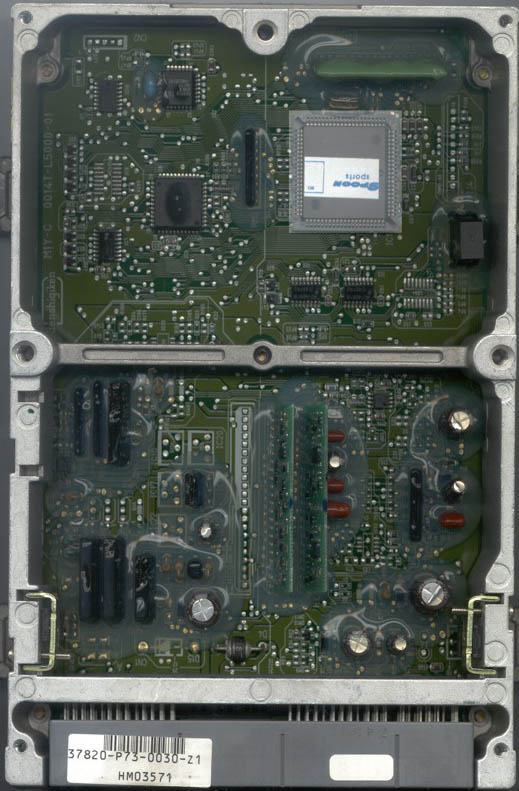
OBD2 Honda ECUs store operating code directly inside the internal ROM of the main microcontrollerâtypically an OKI 66507 series SMT processor. Modification requires replacing this microcontroller entirely with a programmed OKI 66P507 (One-Time Programmable) variant.
1. Hardware Modification & SMT Soldering
Because the factory microcontroller is a surface-mount device (SMD) in a PLCC84 package, standard desoldering pumps are insufficient.
Recommended Chipping Procedure
- Remove the OEM Processor: Desolder the factory OKI 66507 processor from the board. Use a hot-air rework station to evenly heat all 84 pins without lifting the delicate copper pads on the multi-layer PCB.
- Clean the Pads: Clean all solder pads on the PCB using solder wick and flux, ensuring a completely flat surface.
- Install a Socket: Solder a PLCC84 surface-mount socket onto the board. This allows for future swapping of microcontrollers.
- Insert the Modified Processor: Insert a pre-programmed OKI 66P507 into the socket.

2. Programming the OKI 66P507
The OKI 66P507 is an OTP microcontroller and can only be programmed once. To write data using a standard EPROM burner, you must use a custom programming adapter board that maps the PLCC84 pinout to a standard DIP28 layout.
Programming Steps
- Plug the custom adapter into your EPROM burner.
- Place a blank OKI 66P507 MCU into the PLCC socket on the adapter.
- Configure the programming software to target a standard 27C512 EPROM.
- Restrict the target address range to $0000 to $BFFF (representing the 48KB ROM code).
- Set the programming voltage (Vpp) to 12.5V and select a slow programming algorithm.
- Ensure the adapter's configuration jumper is set to position "D" (Data).
- Initiate the programming cycle.
Optional Read Protection
To lock the microcontroller and prevent cloning:
- After successfully writing the data, move the adapter jumper to position "S" (Security).
- Write the value $00 to address $0000. This blows the internal security fuse on the OKI chip.
Warning
Only execute this security step after writing the primary ROM data. If you write to the security address first, the MCU will lock immediately, rendering it permanently unprogrammable.
3. Programming Adapter Reference
For builders constructing their own programming adapter, the following table outlines the mapping between the PLCC84 MCU socket and the DIP28 programmer interface.
VCC
- MCU Pin 1
- DIP28 Pin 28
GND
- MCU Pin 2
- DIP28 Pin 14
A0
- MCU Pin 3
- DIP28 Pin 10
No matching connections.
Tip
Always verify continuity between the PLCC84 socket and the DIP28 header before inserting a blank MCU to prevent hardware damage.