majdi
#31 ◈ 2024-02-25
Re: What components are involved in fuel pump activation del
dj-bobr wrote:
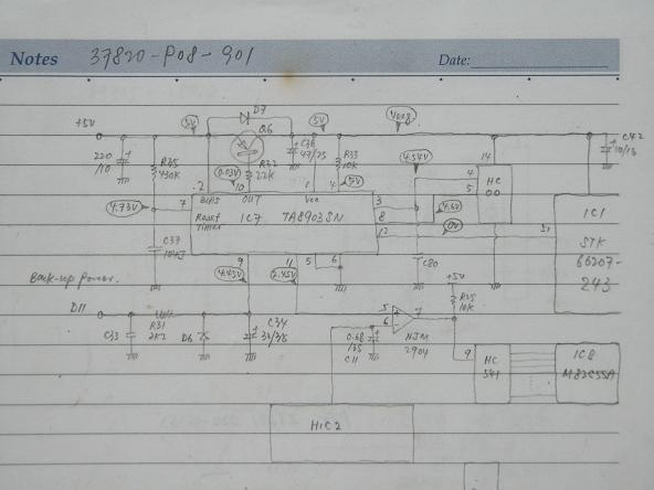
After some ECU repairs during last year, I wonder if IC17 could be bypassed at all when troubleshooting ECUs with fuel pump activation delay (or CEL staying on etc.)
As far as I know, TA8903SN is "power supervisor" IC and it does not deliver power to CPU at all, only information about power status, most likely triggering NMI or RESET.
Anyone interested?
I would appreciate any information about pinout of main OBD1 CPU (M66207) where NMI or RESET pins are, and some brainstorm about the scenario "interrupt PCB path between IC17 and CPU" and "make some Power Good circuit delivering right voltage to NMI and RESET pins to ensure good bootstrap of CPU".
I imagine Power Good circuit as only a pullup resistor to NMI and slight time delayed log. 1 to RESET (so RESET will be lifted few hundreds of milliseconds after Vcc is applied to ECU).
Update: attached M66207 datasheet. NMI is pin 33, RES is pin 29 - the both in inverted logic, as usual in MCUs. Now we have to analyze logic levels during powerup of good ECU and compare with bad ECU with fuel pump delay. Do anyone have logic analyzer?
Also maybe HOLD (pin 34, P2.4) pin is involved somehow - maybe IC17 holds CPU stopped during powerup? (desperately need the logic analysis of NMI, RES and HOLD )
)
As far as I know, TA8903SN is "power supervisor" IC and it does not deliver power to CPU at all, only information about power status, most likely triggering NMI or RESET.
Anyone interested?
I would appreciate any information about pinout of main OBD1 CPU (M66207) where NMI or RESET pins are, and some brainstorm about the scenario "interrupt PCB path between IC17 and CPU" and "make some Power Good circuit delivering right voltage to NMI and RESET pins to ensure good bootstrap of CPU".
I imagine Power Good circuit as only a pullup resistor to NMI and slight time delayed log. 1 to RESET (so RESET will be lifted few hundreds of milliseconds after Vcc is applied to ECU).
Update: attached M66207 datasheet. NMI is pin 33, RES is pin 29 - the both in inverted logic, as usual in MCUs. Now we have to analyze logic levels during powerup of good ECU and compare with bad ECU with fuel pump delay. Do anyone have logic analyzer?
Also maybe HOLD (pin 34, P2.4) pin is involved somehow - maybe IC17 holds CPU stopped during powerup? (desperately need the logic analysis of NMI, RES and HOLD
)The reason the fuel pump start delay is, TA8903 is a voltage regulator with watchdog timer. Some how the internal circuit/capacitor problem. It delay to give 5v output to MCU. To bypass these you just need to replace with modify fixed 5v to the MCU.
and need to solve feedback logic to MCU so it wont trough CEL.