OBD0MPFI
ECUs have two main designs that affect how the
ECU is chipped.
- 90-91 ECUs have an external 38256 (same as 27 C256) ROM. This can be removed and replaced with any of the usual candidates.
- 88-89 ECUs have an Oki83 C154 processor in them and lack the external ROM so easy to replace in the later ECUs.
- 88-91 USDM PM8 (HF) ECUs all use the Oki83 C154 design, even in 90-91.
All is not lost, however. There are THREE ways to chip a 88-89
ECU, and neither are terribly hard:
NOTE to PM7-B020 owners: As
this topic suggests, pin 31 of the
MCU should be disconnected from the
PCB before it is grounded to enable the external
ROM chip. Failing to do so may result in solid
CEL and intermittent
ECU operation. This issue was found only on PM7-B020 and should be considered on other
ECUs only if the normal "jumpering" doesn't work AND there are no faults in adding the socket. This should also not be a problem if you're adding a daughter-board for the
MCU, but yet again, be careful.
1. Replace the 40 pin
MCU with another
Intel8051-compatible
MCU that has
Internal ROM like the
Oki83 C154 and program the
MCU with an
A5-free program. Requires modification of stock programs to remove the weird use of
A5!!! Requires further mods to the program to make it tuly
Intel8051 compatible]
Note: As of 12/Jan/04, this has not been finished.(Current project sez Dave) Requires a programmer that can program the
Intel8051 chip you choose to use. My method of choice. (Dave)
2. Replace the 40 pin
MCU with a daughterboard that has a socket for an
EPROM, a
74 HC373 Latch, a socket for the original
MCU and
_EA setup for an external
ROM instead of internal
ROM. Does not require modification of code - stock program will work fine because
Oki83 C154 is still used. Does require a circuit board, additional parts and significantly more soldering. See also
here
3. This is the easiest way.. You use the same programs as a 90-91.. And install a socket with 6 to 10 inches of wire to each pin. then follow the chart to install the wires from the eprom socket to the board.
| EPROM PINS | MCU PINS(m83c154) | 74hc373 Pins |
| |
| 1 | 40 | |
| 2 | 25 | |
| 3 | | 19 |
| 4 | | 2 |
| 5 | | 16 |
| 6 | | 5 |
| 7 | | 15 |
| 8 | | 6 |
| 9 | | 12 |
| 10 | | 9 |
| 11 | 39 | |
| 12 | 38 | |
| 13 | 37 | |
| 14 | 20 | |
| 15 | 36 | |
| 16 | 35 | |
| 17 | 34 | |
| 18 | 33 | |
| 19 | 32 | |
| 20 | | 10 |
| 21 | 23 | |
| 22 | 29 | |
| 23 | 24 | |
| 24 | 22 | |
| 25 | 21 | |
| 26 | 26 | |
| 27 | 27 | |
| 28 | | 20 |
Pin 31 of M83C154 to pin 20 of M83C154 (Jumper pin) to swicth to the eprom code..
If you will, Pin 31 on the
MCU is the EA (External Addressing) ping, and when you tie it to Pin 20 (GND) you force the
MCU to execute from external
ROM.
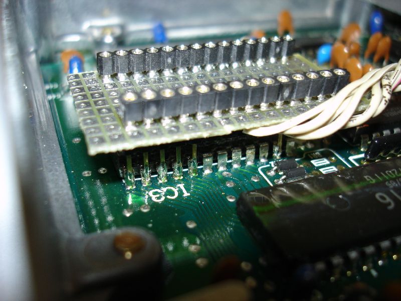
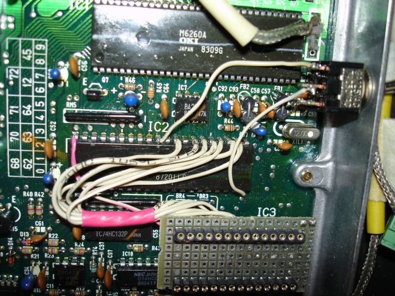
Another possible way of doing this step involves creating a socket for your new chip that sits on top of the External
RAM chip. This approach greatly reduces the wires that need to be used, but the special socket board itself gets a bit triky and may present you with clearance problems ( two chips and a socket on top of each other may stand so tall that you may not be able to mount the top cover of the
ECU). Also, this approach is NOT recommended for people new to soldering. It involves some skills with the iron and a lot of caution.
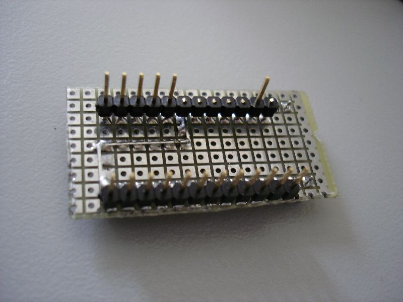
The idea is to mount a socket (
ZIF or not) on a small prototyping board and add 2 single-row headers on the bottom of the board. The headers get soldered to the External
RAM chip, and your newly burned chip goes into the socket. Some of the header pins have to be cut, but you can use a rule of thumb here. Leave only the pins that the table below says are connected to the XRAM. Or just look at the attached pictures to see which ones are missing.
If you get stumbled upon something, Take out the datasheets and triple-check. One more thing i highly recommend is after you're done, check the circuit with a continuity tester, but use the table above! The two tables ARE be electricly identical.
Before you start, examine the photographs I did while chipping my PM6. This will help you get a better picture of what the final thing should look like. I made a small cut on the proto-board to denote PIN1 as is done on most ICs. Also, the below mentioned connection from
EEPROM Pin 28 to Pin 1 was made after the photos were shot, so You will not see it.
| EPROM PINS | MCU PINS(m83c154) | External RAM Pins |
| |
| 1 | 40 | |
| 2 | 25 | |
| 3 | | 1 |
| 4 | | 2 |
| 5 | | 3 |
| 6 | | 4 |
| 7 | | 5 |
| 8 | | 6 |
| 9 | | 7 |
| 10 | | 8 |
| 11 | | 9 |
| 12 | | 10 |
| 13 | | 11 |
| 14 | | 12 |
| 15 | | 13 |
| 16 | | 14 |
| 17 | | 15 |
| 18 | | 16 |
| 19 | | 17 |
| 20 | Connect to EEPROM Pin 14 |
| 21 | 23 | |
| 22 | 29 | |
| 23 | 24 | |
| 24 | 22 | |
| 25 | | 23 |
| 26 | 26 | |
| 27 | 27 | |
| 28 | Connect to EEPROM Pin 1 |
Just to make it clear, Pin 20 of the
EEPROM is connected to
EEPROM pin 14 which (as the table suggests) is connected to
RAM pin12 and therefor it is connected to GND.
EEPROM Pin 28 is connected to
EEPROM pin 1 and they both are connected to the
MCU pin40 which is the +5V Vcc.
And don't forget to connect "Pin 31 of M83C154 to pin 20 of M83C154 (Jumper pin) to swicth to the eprom code..."
| Attachment: | Modify: | Size: | Date: | Who: | Comment: |
|---|
 DSC00663.jpg DSC00663.jpg | mod | 65387 | 10 May 2005 - 13:47 | 1net | Socket Board ( Top) |
| DSC00662.jpg | mod | 67627 | 10 May 2005 - 13:48 | 1net | Socket Board ( Bottom) |
| DSC00667.jpg | mod | 99145 | 10 May 2005 - 13:49 | 1net | Soldered Socket Board 1 |
| DSC00672.JPG | mod | 125029 | 10 May 2005 - 13:50 | 1net | Soldered Socket Board 2 |
| DSC01263_small.jpg | mod | 157074 | 17 Aug 2005 - 06:45 | 1net | Soldered Socket Board 3 ( all done) |