OBD0 ECU Chipping and ROM Modification (1988–1989)
Archived methods for socketing and chipping early OBD0 Honda and Acura ECUs (1988–1989) with internal ROM, including flywire and piggyback EPROM installation techniques.
Most OBD0 MPFI ECUs from 1990â1991 use external ROM cartridges compatible with the 38256 standard, which can be easily removed and replaced. Many 1988â1989 units, however, integrate ROM directly into the OKI M83C154 microprocessor. This guide documents three archived modification approaches for these internal-ROM designs, applicable to all USDM PM8 HF ECUs from 1988â1991.
Warning
Disconnect the ECU from the vehicle before soldering. Verify every connection with a continuity test and check for short circuits before applying power.
Enabling External ROM Access
To execute code from an external ROM, connect Pin 31 (_EA, the external access pin on the M83C154) to Pin 20 (ground) on the MCU.
Warning
On PM7-B020 boards, sources indicate that Pin 31 must first be isolated from the PCB before connecting it to ground. Failure to do so has caused permanent check engine lights (CEL) and intermittent operation. Consider this isolation step on other boards only if standard jumper placement fails and socket connections show no faults.
Three Documented Approaches
1. MCU Replacement
Replace the 40-pin OKI MCU with a compatible Intel 8051-based microprocessor containing internal ROM.
Considerations:
- Requires modifying firmware to remove
A5instruction usage and ensure Intel 8051 compatibility - Requires a dedicated programmer for the replacement MCU
- Status: This approach was incomplete as of January 2004
2. Daughterboard with Integrated Address Latch
Replace the 40-pin MCU with a daughterboard containing:
- A socket for the original OKI MCU
- An address latch (
74HC373) - An external EPROM socket
- Hardware to configure
_EAfor external ROM operation
Advantages:
- Preserves the original OKI MCU, eliminating firmware modification requirements
- Requires fewer software changes than MCU replacement
Disadvantages:
- Requires custom PCB fabrication, additional components, and extensive soldering
3. External EPROM via Flywire or Piggyback
Mount a 28-pin EPROM socket and wire it directly to the MCU and address latch. Two wiring methods are documented: direct flywire and XRAM piggyback overlay.
Flywire Pinout Map
| EPROM Pin | MCU M83C154 Pin | 74HC373 Pin | Notes |
|---|---|---|---|
| 1 | 40 | â | +5V |
| 2 | 25 | â | |
| 3 | â | 19 | Address bus |
| 4 | â | 2 | Address bus |
| 5 | â | 16 | Address bus |
| 6 | â | 5 | Address bus |
| 7 | â | 15 | Address bus |
| 8 | â | 6 | Address bus |
| 9 | â | 12 | Address bus |
| 10 | â | 9 | Address bus |
| 11 | 39 | â | Data bus |
| 12 | 38 | â | Data bus |
| 13 | 37 | â | Data bus |
| 14 | 20 | â | Ground |
| 15 | 36 | â | Data bus |
| 16 | 35 | â | Data bus |
| 17 | 34 | â | Data bus |
| 18 | 33 | â | Data bus |
| 19 | 32 | â | Data bus |
| 20 | â | 10 | Control signal |
| 21 | 23 | â | Control signal |
| 22 | 29 | â | Control signal |
| 23 | 24 | â | Control signal |
| 24 | 22 | â | Control signal |
| 25 | 21 | â | Control signal |
| 26 | 26 | â | Control signal |
| 27 | 27 | â | Control signal |
| 28 | 40 | â | +5V (see note below) |
Important
The archived flywire table lists MCU Pin 20 for EPROM Pin 28, but a clarification on the same source states that both EPROM Pins 28 and 1 connect to MCU Pin 40 (+5V). MCU Pin 20 is identified as ground elsewhere on the page. Verify the circuit before making connections.
XRAM Piggyback Overlay Pinout Map
The alternative method mounts the EPROM socket on a small prototype board stacked directly over the external RAM. Warning: Stacked mounting can cause clearance issues and is not recommended for soldering beginners.
| EPROM Pin | MCU M83C154 Pin | External RAM Pin | Notes |
|---|---|---|---|
| 1 | 40 | â | +5V |
| 2 | 25 | â | |
| 3 | â | 1 | Address bus |
| 4 | â | 2 | Address bus |
| 5 | â | 3 | Address bus |
| 6 | â | 4 | Address bus |
| 7 | â | 5 | Address bus |
| 8 | â | 6 | Address bus |
| 9 | â | 7 | Address bus |
| 10 | â | 8 | Address bus |
| 11 | â | 9 | Address bus |
| 12 | â | 10 | Address bus |
| 13 | â | 11 | Address bus |
| 14 | â | 12 | Address bus |
| 15 | â | 13 | Address bus |
| 16 | â | 14 | Address bus |
| 17 | â | 15 | Address bus |
| 18 | â | 16 | Address bus |
| 19 | â | 17 | Address bus |
| 20 | Connect to EPROM Pin 14 | â | Ground reference |
| 21 | 23 | â | Control signal |
| 22 | 29 | â | Control signal |
| 23 | 24 | â | Control signal |
| 24 | 22 | â | Control signal |
| 25 | â | 23 | Data bus |
| 26 | 26 | â | Control signal |
| 27 | 27 | â | Control signal |
| 28 | Connect to EPROM Pin 1 | â | +5V |
Important
Pin connections for XRAM piggyback: EPROM Pin 20 connects to both EPROM Pin 14 and RAM Pin 12 (ground). EPROM Pins 28 and 1 both connect to MCU Pin 40 (+5V). Connect MCU Pin 31 to MCU Pin 20 to select external ROM operation.
Piggyback Installation Gallery
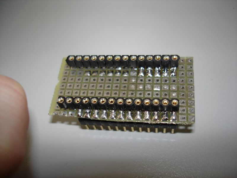 Top view of the EPROM socket daughterboard.
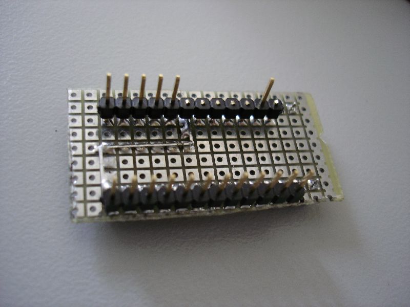 Bottom view of the EPROM socket daughterboard.
 Header pins soldered to the external RAM module.
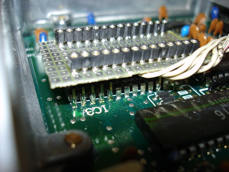
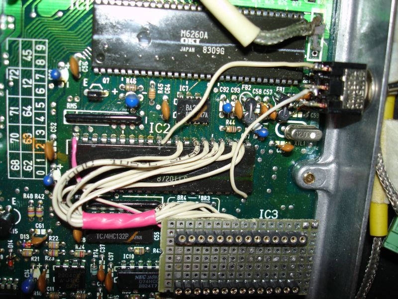 Fully wired XRAM external connections.
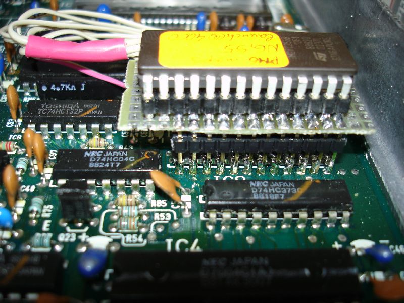 Final piggyback installation mounted on the ECU PCB.