P30 JDM D12 Analog Input Modification
Archived P30 JDM D12 circuit modification to log a 0–5 V analog input through the ECU via an unused pin.
This archived modification utilizes the otherwise unused D12 input on a P30 OBD1 JDM ECU to log a 0â5 V analog signal, such as the output from an EGT thermocouple amplifier.
Warning
This procedure cuts or alters ECU board circuits. The source reports successful testing on P30 USDM and JDM units but does not establish compatibility with other OBD1 ECUs. Verify the circuit and software behavior before modifying an ECU.
USDM vs. JDM P30 Differences
The original investigation tested on a P30 USDM unit initially and a P30 JDM unit for modification and testing. Other Honda OBD1 ECUs were expected to be similar, but this was not confirmed.
| Detail | USDM P30 | JDM P30 |
|---|---|---|
| D12 components | All installed | Some components missing |
| D12 circuit | Described as simpler | Described as more complex |
| D12 analog input | AI3, pin 57 of 66207 in 64-pin DIP package |
AI5, pin 63 of 66207 in 68-pin PLCC package |
| Analog input grounded | AI5, pin 59 of 66207 |
AI3, described as pin 61 of 66207 |
| ADC upper eight bits | RAM 067h |
RAM 06Bh |
| Remaining two ADC bits | MSBs of RAM 066h as two LSBs of ADC value |
MSBs of RAM 06Ah as two LSBs of ADC value |
Note
The archived JDM section references "USDM" twice when describing the JDM circuit: designating the grounded AI3 input as part of a USDM P30, and labeling the D12-to-AI5 path as "USDM D12 wiring." The table above follows the surrounding JDM context, but these designations were not independently corrected or verified.
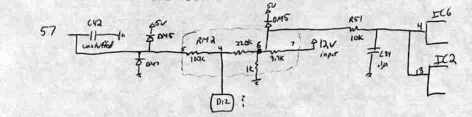 Archived schematic of the USDM P30 D12 circuit.
Archived JDM Modification
The source indicates all alterations are made on the back of the ECU board:
- Replace
R15with a diode. - Install a diode at
R14. The source used surface-mount (SMD)1N4148diodes and described them as protection for the66207analog input. - Add a jumper at
R13. - Add a jumper between the ungrounded connections of
Q3to route D12 to the modified circuit. - Leave
R16(33 kΩ) andC17unchanged. The source did not identify the value ofC17and noted it appeared to be a tantalum capacitor.
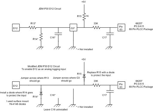 Archived before-and-after schematic for the P30 JDM D12 modification.
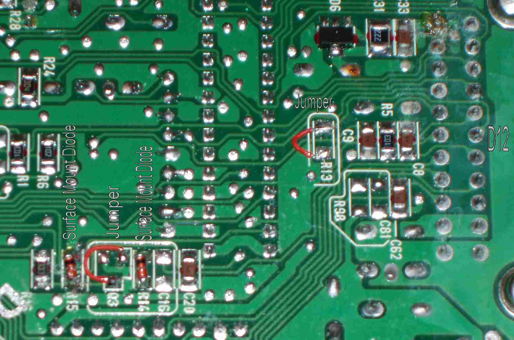 Archived high-resolution photo of the modified P30 JDM board.
The author tested both P30 variants using a 10 kΩ potentiometer as a variable voltage divider on a 5 V supply, and with an EGADS EGT sensor. These tests do not confirm operation with other sensors or ECU variants.
Software Warning for AI5
The archived page warns that OBD1 code appears to read AI5 and execute an unidentified function. Until that code was understood, a different and more invasive arrangement was proposed:
- Cut traces to AI3 and AI5 on the
66207. - Ground AI5.
- Route the D12 circuit to AI3.
The source expected this pin swap to make a JDM ECU log D12 as a USDM ECU would. It did not document the unknown AI5 function and provided no broader validation, so treat this as an unverified historical proposal rather than a current recommendation.