Chipping 1988-1989 OBD0 ECUs
Archived socketing and chipping methods for early 1988-1989 Honda and Acura OBD0 ECUs.
Adapted from pgmfi.org wiki
Most 1990-1991 OBD0 MPFI ECUs use an external 38256-compatible ROM that can be removed and replaced. Many 1988-1989 ECUs instead use an OKI M83C154 processor with internal ROM. The archived guide also says all 1988-1991 USDM PM8 HF ECUs use this internal-ROM design.
This article preserves the three modification approaches and two wiring tables described by the original pgmfi community.
Warning: Disconnect the ECU from the vehicle before soldering. Verify every connection with a continuity tester and check for shorts before applying power.
Enabling external ROM access
The guide says to connect Pin 31, the M83C154 external-access (_EA) pin, to Pin 20
(ground) so the MCU executes code from an external ROM.
Warning: On PM7-B020 boards, the source says MCU Pin 31 must be disconnected from the PCB before it is grounded. It reports a solid CEL and intermittent operation when that pin remains connected. The source says to consider this on other boards only when normal jumpering fails and the socket wiring has no faults.
Three documented approaches
1. Replace the MCU
Replace the 40-pin OKI MCU with an Intel 8051-compatible MCU containing internal ROM.
The archived guide says this requires modifying the program to remove its use of the
A5 instruction and making further changes for Intel 8051 compatibility. It also
requires a programmer for the replacement MCU.
The source noted in January 2004 that this approach was not finished.
2. Install an MCU daughterboard
Replace the 40-pin MCU with a daughterboard containing:
- A socket for the original OKI MCU
- A
74HC373address latch - An external EPROM socket
- Hardware that configures
_EAfor external ROM
This approach keeps the original OKI MCU and therefore does not require the same program changes, but it requires a circuit board, additional components, and more soldering.
3. Wire an external EPROM
Install a 28-pin EPROM socket and connect it to the MCU and address latch. The source describes a direct flywire method and an XRAM piggyback method.
Flywire mapping
This table is a direct pin mapping from the archived page.
| EPROM pin | M83C154 MCU pin | 74HC373 pin |
|---|---|---|
| 1 | 40 | - |
| 2 | 25 | - |
| 3 | - | 19 |
| 4 | - | 2 |
| 5 | - | 16 |
| 6 | - | 5 |
| 7 | - | 15 |
| 8 | - | 6 |
| 9 | - | 12 |
| 10 | - | 9 |
| 11 | 39 | - |
| 12 | 38 | - |
| 13 | 37 | - |
| 14 | 20 | - |
| 15 | 36 | - |
| 16 | 35 | - |
| 17 | 34 | - |
| 18 | 33 | - |
| 19 | 32 | - |
| 20 | - | 10 |
| 21 | 23 | - |
| 22 | 29 | - |
| 23 | 24 | - |
| 24 | 22 | - |
| 25 | 21 | - |
| 26 | 26 | - |
| 27 | 27 | - |
| 28 | 20 in source table; see note | - |
Note: The archived flywire table lists MCU Pin 20 for EPROM Pin 28, but a later clarification on the same page says EPROM Pins 28 and 1 both connect to MCU Pin 40 (+5 V). Pin 20 is identified as ground elsewhere on the page. Verify the circuit before wiring.
XRAM piggyback mapping
The alternative method mounts the EPROM socket on a small prototyping board above the external RAM. The source warns that the stacked assembly can cause clearance problems and does not recommend this method for people new to soldering.
| EPROM pin | M83C154 MCU pin | External RAM pin |
|---|---|---|
| 1 | 40 | - |
| 2 | 25 | - |
| 3 | - | 1 |
| 4 | - | 2 |
| 5 | - | 3 |
| 6 | - | 4 |
| 7 | - | 5 |
| 8 | - | 6 |
| 9 | - | 7 |
| 10 | - | 8 |
| 11 | - | 9 |
| 12 | - | 10 |
| 13 | - | 11 |
| 14 | - | 12 |
| 15 | - | 13 |
| 16 | - | 14 |
| 17 | - | 15 |
| 18 | - | 16 |
| 19 | - | 17 |
| 20 | Connect to EPROM Pin 14 | - |
| 21 | 23 | - |
| 22 | 29 | - |
| 23 | 24 | - |
| 24 | 22 | - |
| 25 | - | 23 |
| 26 | 26 | - |
| 27 | 27 | - |
| 28 | Connect to EPROM Pin 1 | - |
The source clarifies that EPROM Pin 20 connects to EPROM Pin 14 and RAM Pin 12 for ground, while EPROM Pins 28 and 1 connect to MCU Pin 40 for +5 V. It again says to connect MCU Pin 31 to MCU Pin 20 to select external ROM.
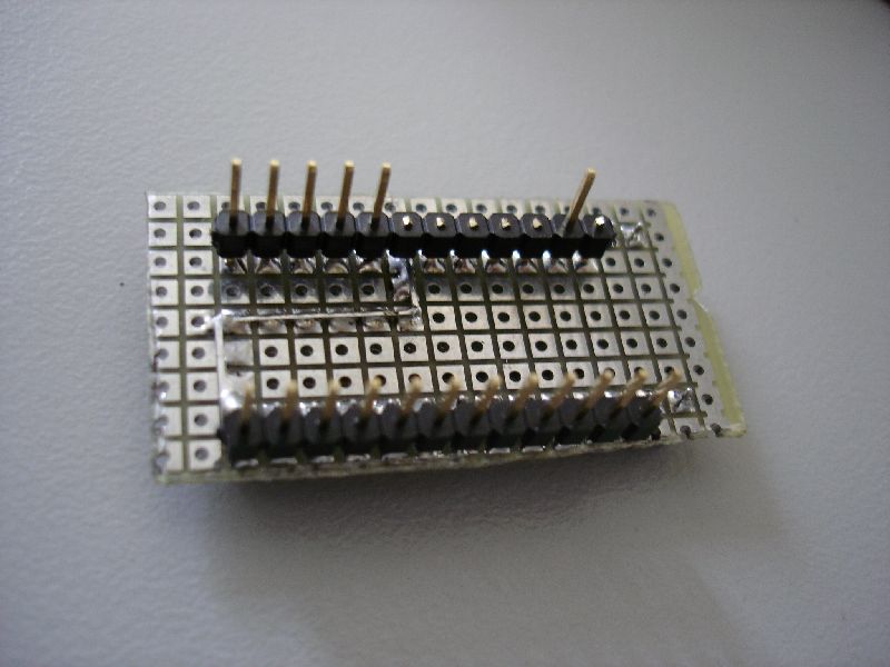
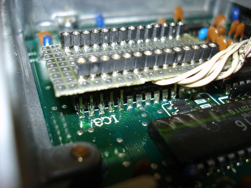
Piggyback installation photos
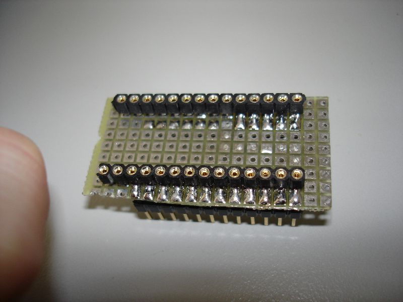 Daughterboard socket, top view.
 Daughterboard socket, bottom view.
 Header pins soldered to the external RAM.
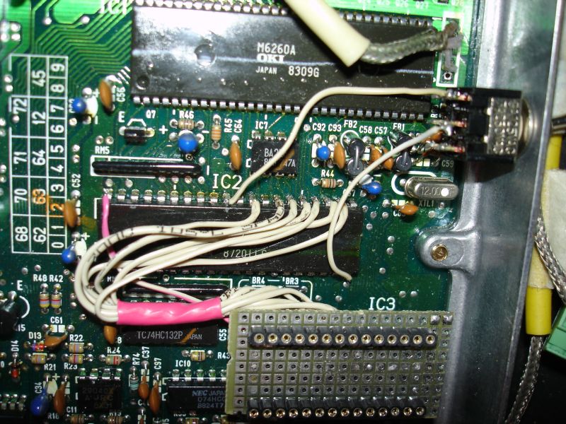 Completed XRAM connections.
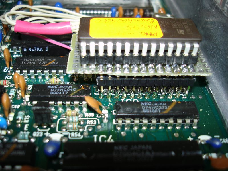 Completed installation stacked on the ECU board.
Credits and source
Authors blundar, crxsirvtec, 1net
Source Adapted from Chipping An88-89ECU on pgmfi.org wiki. Licensed under CC BY-NC-SA 1.0.